Sony Creates 1,000 fps HD CMOS for Smartphones

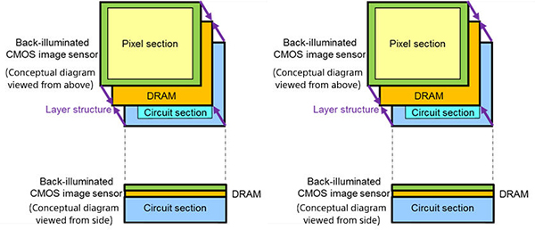
TOKYO—Sony Corp. today announced the development of a 1,000 fps stacked CMOS designed for smartphones. The new image sensor consists of a DRAM layer added to the conventional two-layer stacked CMOS image sensor, with a layer of back-illuminated structure pixels and a chip affixed with mounted circuits for signal processing. (See graphic below.)
Sony said this newly developed sensor with DRAM delivers fast data readout speeds, making it possible to capture still images of fast-moving subjects with minimal focal plane distortion as well as super slow-motion movies at up to 1,000 frames per second in 1,920x1,080-pixel HD.
To get the high-speed readout, Sony said the circuit used to convert the analog video to a digital signal was doubled from a two-tier to a four-tier construction to improve processing ability.
Although there are speed limitations in the interface specs for outputting signals from image sensors to other LSIs, this sensor uses DRAM to temporarily store signals read at high speed, enabling data to be output at an optimal speed for the standard specs. As a result, Sony said the product is capable of reading one still image of 19.3 million pixels in 1/120 of a second, supporting high-speed image capture.
The sensor is also said to include technology for reducing the noise generated between the circuits on each of the three layers.
The sensor results were announced at the International Solid-State Circuits Conference, which started on Sunday, Feb. 5, 2017 in San Francisco, Sony said.

Get the TV Tech Newsletter
The professional video industry's #1 source for news, trends and product and tech information. Sign up below.
