What Comes After Silicon?

Let's talk about silicon—semiconductors, that is.
The concept of the transistor dates back to at least 1925, when a physicist named Julius Edgar Lilenfeld obtained a Canadian patent for a field-effect transistor. He later obtained U.S. patents for the same device, although he never published any papers about the device or described a working model. In 1947, Bell Telephone Labs devised a working germanium transistor, and in 1951, announced a working junction transistor. The prototypes were of course considerably larger than the vacuum tubes they eventually replaced, and the early production devices were quite fragile electrically. I remember as a young lad experimenting with and learning about radio and electronics in the 1950's, thinking that transistors probably did not have much of a future. Oh well.
Doped silicon semiconductors have for decades been the basis of the ever more complex and powerful electronics that have become such a central part of our lives, both personal and professional. In 1960, an electrical engineer named Douglas Engelbart proposed the idea that if the basic circuitry of digital computers, which then consisted of vacuum tubes, could be reduced in size, this could lead to a dramatic increase in their power.
MOORE'S LAW
We are all familiar with a lithographic chemist named Gordon Moore, who in 1965 stated in an article in "Electronics," that the number of components that could be incorporated per integrated circuit would increase exponentially over time. This became known as Moore's Law. Since 1970, the number of components per chip of a given size has doubled every two years. This has produced a "virtuous cycle," in which the size, component density, and power of electronic devices has steadily increased. According to "More Than Moore," a white paper published by the International Technology Roadmap for Semiconductors (ITRS), in 1954, five years before the integrated circuit was invented, the average price of a transistor was $5.52. By 2004, the price had dropped to a billionth of a dollar per transistor.

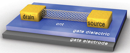
An "idealized" carbon nanotube field effect transistor Computer processor chips are comprised of complementary metal oxide semiconductor (CMOS) devices, which were called complementary-symmetry metal oxide semiconductors or "cos-mos," by their inventor, RCA. CMOS transistors use considerably less power than bipolar transistors, making the exponentially increasing numbers of transistors practical, up to a point. But the doubling of the density of CMOS transistor fabrication every two years has reached the point at which real limits have appeared. In 2011 the target semiconductor feature size shrank from the 2009 target of 32 nanometers (32 x 10-9 meter) to 22 nanometers. At 32 nanometers, the gate oxide thickness is 1.2 nanometers, or 5 silicon atoms thick. At this point, electron tunneling through short channels, thin insulator films and their associated leakage currents, ever-increasing clock speeds, and other effects have led to increased fabrication costs and the generation of a furious amount of heat. Ten years ago, Intel's chief technology officer warned that if trends continued in the way they had been going, by 2011, microprocessor chips would reach the surface temperature of the sun.
CARBON NANOTUBE TRANSISTORS
One technology that is being explored as a replacement for today's semiconductors is the use of carbon nanotubes to make carbon nanotube field-effect transistors, or CNFETs. Carbon atoms are found in four different allotropes, or structural forms. The atoms may be bound in tetrahedral lattices, in which form they are known as diamond; in multiple sheets of hexagonal lattices, in which form they are known as graphite; in the form of graphene, which is a single sheet of graphite; or as fullerenes, where the atoms are bound together in spherical, tubular, or ellipsoid formations.
Graphene is a single sheet of carbon bound in the form of a hexagonal lattice resembling a tiny chicken-wire sort of structure that has the unique property that it can roll up, forming a hollow cylinder a few atoms wide (see Fig. 1). Owing to quantum mechanics, depending on the angle at which the graphene is cut from the sheet, the resulting nanotube has a particular chirality, or "twist," which chirality gives the nanotube electrical properties ranging from metallic conduction, to semiconduction, to a small gap. A semiconducting nanotube is placed on a substrate, with gold forming the contacts: the sources, gates, and drains of the field effect transistors. It is hoped that within the next five years this method will produce semiconductors whose feature size is as small as 7 nanometers.
The world as we know it has become dependent on digital devices of ever increasing complexity and power. Somewhat ironically, this boils down to making a lot of ever smaller and ever faster on/off switches. Practical carbon nanotube transistors could keep this game running for a few more Moore's Law cycles, which will give us more time to come up with the next step. Of course, when we reach the point where we can make single-atom digital switches, that would appear to be the end of it. Unless we can devise a quark switch.
Randy Hoffner is a veteran of the big three TV networks. He can be reached through TV Technology.
Get the TV Tech Newsletter
The professional video industry's #1 source for news, trends and product and tech information. Sign up below.

